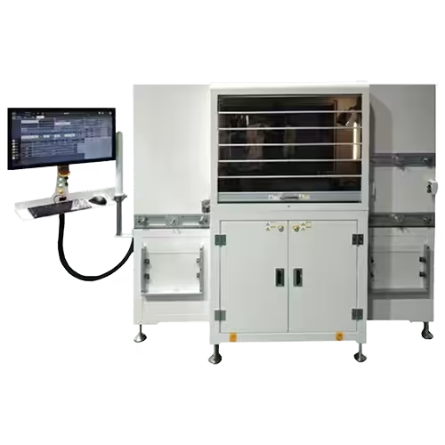
SWIReR45 SWIR Vision System
Advanced Semiconductor Defect Detection with Micron-Level Precision
The SWIReR45 integrates cutting-edge Short-Wave Infrared (SWIR) imaging with deep-learning AOI to detect critical defects invisible to conventional vision systems. Consequently, it ensures precise detection of internal cracks, sidewall chipping, and surface anomalies—even on ultra-thin, low-transmittance dies—while maintaining exceptional throughput and image quality.
Identifying Hidden Defects Before They Escalate
Reduce production risk and improve final yield
In high-value semiconductor packaging, hidden structural damage often originates during wafer dicing or the pick-and-place (P&P) process. While sidewall cameras may capture longitudinal cracks, they typically fail to detect transverse cracks and corner chipping. This limitation can result in undetected defects reaching downstream assembly stages, potentially leading to costly rework or field failures.
Furthermore, ultra-thin chips (<100 µm) often lack legible markings, making orientation detection critical. By employing SWIReR45’s advanced SWIR imaging, manufacturers can reliably detect these defects early, thereby preventing yield loss and safeguarding customer quality standards.
Why SWIR Imaging?
Harnessing the Penetration Power of SWIR Technology
Operating at wavelengths between approximately 1,000 and 1,700 nm, SWIR penetrates materials such as bare silicon and certain backside-coated dies with superior clarity compared to visible and near-infrared (NIR) imaging. As a result, defect edges become more distinct, enabling more accurate automated optical inspection (AOI).
Higher contrast, greater reliability, and safer integration than X-ray
Unlike X-ray systems, SWIR does not require radiation safety infrastructure, significantly reducing operational complexity and cost. More importantly, it delivers high-contrast imagery in real time, making it an optimal solution for automated visual inspection (AVI) lines where speed and reliability are paramount.
Competitive Strengths
- Zero missed detections with ultra-low false reject rates.
- Custom-engineered mechanical design for stability and throughput.
- Proprietary SWIR camera developed for semiconductor inspection.
- Custom optical lens assembly for maximum light efficiency.
- Patented high-speed autofocus system (< 50 ms).
- Deep-learning AOI integration for adaptive defect detection.
- Wide application range across various die types and package formats.
- High-speed inspection without sacrificing detection accuracy.
Four “Mosts” of SWIReR45
- Largest Field of View: 3.21 mm × 2.57 mm (competitors: 2.2 mm × 2 mm).
- Fastest Throughput: UPH up to 80K—speed advantage increases with larger die sizes.
- Highest Image Contrast: Clear separation of defects from background, including hard-to-see inner cracks.
- Finest Detection Precision: 1.25 µm/pixel resolution with 6 µm × 6 µm minimum defect size detection.
SWIReR45 Technical Features
High Efficiency & Wide Defect Handling
- Pattern comparison – detects layout deviations and structural misalignments.
- 180° rotation detection – ensures correct die orientation even without markings.
- Surface cracks – identifies micro-fractures visible on the surface.
- Internal cracks – uncovers sub-surface fractures hidden from standard cameras.
- Sidewall chipping – locates edge damage affecting mechanical integrity.
- Corner chipping – captures small but critical corner defects.
Camera
5.24 Mega Pixel
Light Source
Short Wavelength Infra Red (SWIR)
Work Stations
2 Each
UPH (1×1 mm)
> 50K
Auto Focus
Patented High-Speed (< 50 ms)
Detection Capability
> 6 µm
Overkill Rate
< 1%
Image Quality—Precision Starts with Superior Image Quality
The SWIReR45 enforces strict image quality criteria to ensure AOI and AI algorithms operate at maximum accuracy:
- Resolution: Pixel size equals one-fifth to one-tenth of the smallest detectable defect.
- Contrast: Gray-level difference between background and feature ≥ 30 (recommended ≥ 50).
- Sharpness: No blurring at edges—indicating correct focus.
- Cleanliness: Absence of foreign marks or grinding traces outside defect areas.
- Noise Control: Camera gain and parameters optimized to prevent false positives.
By meeting these standards, SWIReR45 delivers consistent, reliable defect classification while minimizing false detections.
Integration with CosX Vision Ecosystem
The SWIReR45 is engineered for seamless deployment alongside other CosX inspection and packaging solutions. Its inline-ready architecture allows integration into high-volume production lines, complementing solder ball mount, BGA repair, and die bonding systems.
This ensures a holistic defect detection ecosystem, reducing rework costs and safeguarding long-term reliability.