Vision
Vision Systems for Advanced Semiconductor Inspection
Our vision systems combine state-of-the-art imaging technologies with AI-driven analysis to detect defects that traditional inspection methods often miss. Whether inspecting at the micron level or revealing hidden cracks deep within materials, our solutions deliver uncompromising accuracy, speed, and reliability for semiconductor manufacturing.
Precision Inspection for a Defect-Free Future
As semiconductor devices become smaller, thinner, and more complex, the margin for error has never been tighter. Traditional optical inspection tools often fail to detect sub-surface defects, micro-cracks, and orientation errors that can compromise product performance and yield.
Our vision systems are purpose-built for high-value manufacturing, delivering:
- Micron-level defect detection for even the smallest anomalies
- High-speed throughput to keep pace with modern production lines
- Deep-learning AI integration for adaptive, intelligent inspection
- Material-penetrating imaging such as SWIR for hidden defect detection
Innovating Across Inspection Modalities
We offer specialized systems tailored to different inspection needs, from surface defect detection to advanced sub-surface imaging. Each system is engineered with precision optics, advanced sensors, and intelligent software to ensure maximum reliability and repeatability in high-volume manufacturing environments.
Your Partner in Precision Inspection
Choosing the right vision system means balancing detection capability, speed, and integration flexibility. Our systems are designed to work seamlessly with your production lines, offering full SECS/GEM compatibility, real-time data backup, and robust mechanical stability.
From proof-of-concept trials to full-scale deployment, we provide the expertise and technology to ensure your inspection process exceeds industry standards.
Featured Model
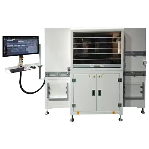
SWIReR45 – SWIR Vision System for Hidden Defect Detection
The SWIReR45 is our flagship SWIR-based vision system, purpose-built for detecting internal cracks, sidewall chipping, and micro-defects that conventional cameras cannot see. Operating at 1,000–1,700 nm, it penetrates materials like bare silicon and backside-coated dies to deliver high-contrast, high-resolution imagery at industry-leading speeds.
Key Features:
- Patented high-speed autofocus (< 50 ms)
- Detection capability down to 6 µm
- Large Field of View
- Ultra-low overkill rate (< 1%)
Ensuring Semiconductor Reliability with Vision
CosX Vision Inspection empowers manufacturers to reduce risk, improve quality, and accelerate innovation in advanced packaging.